Introduction
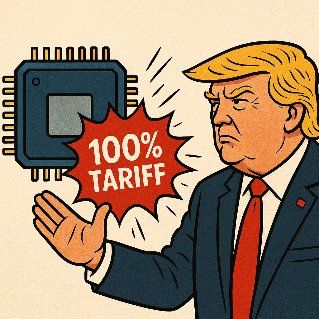
The United States is signaling a hard reset on where the brains of modern electronics get made. The administration has announced its intent to levy a 100 percent tariff on imported semiconductors, paired with a clear escape route for companies that manufacture in the United States or make substantial, verifiable commitments to do so. The message to the market is simple: if you plan to sell a lot of chips into America, you will either pay a steep price at the border or you will stand up serious capacity on U.S. soil.
Chips are the silent ingredient in daily life. Phones, laptops, cars, aircraft, medical devices, factory robots, solar inverters, smart meters, data centers, and refrigerators all depend on integrated circuits. When semiconductor supply faltered during the pandemic, assembly lines slowed, product launches slipped, and everyone was reminded how fragile the global tech stack can be. It is not surprising that Washington wants more of that stack closer to home. What follows is a practical, experience-driven guide to what the tariff does, what “building in the United States” will likely mean in practice, where the gray areas sit, and how both large and small teams can prepare.
What a 100 Percent Tariff Actually Does
A 100 percent tariff doubles the declared value of covered semiconductor imports at the moment they cross the border. If a shipment of packaged microcontrollers is valued at ten million dollars, Customs would assess another ten million dollars before the parts clear. In financial reporting, that extra amount becomes part of the landed cost. Landed cost then flows into a bill of materials, device pricing, and ultimately a retail tag. Procurement teams model those pass-through effects fast. So do product managers who must decide whether to absorb margin pressure, raise prices, redesign a board, or pull demand forward ahead of an implementation date.
The market impact will vary by chip class. Commoditized microcontrollers and analog parts can see price elasticities bite immediately because alternatives exist. High performance processors and leading-edge accelerators are harder to substitute, so tariffs are more likely to show up in final product pricing. Packaging-heavy devices that rely on advanced 2.5D or 3D integration could face compounded effects if assembly and test sit offshore while die are sourced from multiple countries.
What Counts as Building in the United States
Semiconductor production is a journey with many gates. It starts with design and runs through wafer fabrication, assembly, test, and packaging. Each step breaks down further. Wafer fabrication includes front end processes like deposition, lithography, etch, implant, and metrology, followed by back end of line steps that create the metal interconnects.
Assembly and test range from wire bond and conventional molding to advanced fan-out, through-silicon vias, chiplets, and co-packaged optics. Some stages demand massive capital outlays, cleanroom infrastructure, and rare skills. Others are more modular and can be relocated faster. Because the process is multi-stage, the definition of “building in the United States” matters. Expect criteria to center on the following elements.
Domestic value creation
Regulators typically look for meaningful value add inside the country. In chips, that could mean wafer fabrication on U.S. soil for a given node, or advanced packaging performed domestically at commercial scale. Merely relabeling or repackaging a finished device without substantive process steps rarely counts.
Traceability and verifiable milestones
Announcements alone do not satisfy compliance. Companies will be expected to produce verifiable evidence: site selection agreements, building permits, construction progress, equipment purchase orders, tool installation reports, production qualification runs, and first commercial shipment documents.
Capacity that serves the U.S. market
A carveout will likely ask whether U.S. facilities meaningfully serve American demand. Capacity reserved for export may not qualify. Expect questions about allocated wafer starts, packaged unit volumes, and long-term supply agreements with domestic customers.
Workforce and operating plans
Facilities need trained people. Compliance files that include apprenticeship programs, university partnerships, and evidence of sustained hiring plans signal seriousness. Staffing a pilot line for photo-ops will not pass muster if the factory does not ramp.
The Escape Hatch: What a Qualifying Commitment Could Look Like
The administration has signaled a pathway for companies that manufacture domestically or commit to do so. Based on how similar policies are enforced, a robust commitment will have concrete features.
Shovel in the ground, tools on order
Regulators respond to hard facts. A qualifying plan usually includes a signed construction contract, a detailed equipment list with vendor purchase orders, and delivery schedules for scanners, deposition tools, etchers, testers, and packaging lines. The more specific the tooling, the stronger the claim.
Stage-gated production timeline
A credible ramp plan lays out engineering milestones: shell complete, cleanroom certification, first tool install, line bring-up, process qualification, and yield targets. Publishing quarterly gates with objective metrics keeps everyone honest.
Volume and mix aligned to U.S. needs
It is not enough to promise a factory. The commitment should align named products and volumes to domestic customers. That may include binding supply agreements that dedicate a portion of wafer starts or packaged units to the U.S. market for a defined period.
Audit-ready documentation
Build a compliance file as if a customs auditor will ask for it tomorrow. Include chain-of-custody records for wafers and packaged units, traveler logs for process steps, and independent validation where possible. Digital traceability from die to device simplifies audits and reduces business risk.
Gray Areas and Practical Questions Companies Are Already Asking
Policy announcements move fast. Product roadmaps do not. Here are the questions teams are debating in war rooms right now.
Does design alone qualify
Chip design is a high-value activity, and the United States is a design powerhouse. However, most tariff regimes focus on where manufacturing steps occur. Expect that design alone will not satisfy the domestic production standard unless coupled with U.S. fab or packaging activity.
What about advanced packaging
The industry’s shift toward chiplets and 3D stacking puts packaging at center stage. If your die are fabricated abroad but you perform high-value advanced packaging and final test in the United States, you may be within the spirit of the rule. The outcome will hinge on how “substantial transformation” is defined for semiconductors in the implementation guidance.
Are development lots enough
Engineering runs and pilot lots are part of standing up capacity, but they are not a substitute for commercial volume. If your compliance plan rests on small test batches with no path to scale, assume it will face scrutiny.
How do retroactive claims work
Announcements have referenced retroactive assessments for firms that claim domestic plans but fail to execute. Companies should be conservative: do not book exemptions against future milestones unless contracts, financing, and permits are locked.
Cost, Pricing, and Supply Chain Scenarios
Experienced operators will model scenarios along three axes: time to qualification, tariff exposure by product, and redesign feasibility.
Short term: price pressure and selective redesign
In the first two to four quarters after a tariff takes effect or looks imminent, expect procurement to blend strategies. High-margin products may absorb some cost while low-margin SKUs see board-level redesigns that swap vulnerable parts for domestic equivalents. Expect distributor inventories to turn quickly as teams pull forward buys ahead of key dates.
Medium term: packaging migration and dual-sourcing
OSAT providers will sprint to stand up U.S. lines for advanced packaging and final test. Meanwhile, device makers will dual-source key components: a domestic variant for U.S. builds and an offshore variant for other regions. This complicates validation and firmware support, so set aside budget for sustained engineering.
Long term: rebalanced ecosystems
If policy stays consistent, wafer fabrication, packaging, materials, and tool ecosystems will deepen in the United States. University programs will expand and workforce pipelines will thicken. Lead times for highly specialized tools remain a constraint, so plan for staggered ramps and maintain contingency capacity in friendly markets.
Step-by-Step: How To Prepare Your Compliance and Operating Plan
The best compliance plan is built into your operations rather than stapled on top of them. Treat the following as a practical checklist.
Map your exposure by product family
Tag every part number in your bill of materials with origin, packaging location, and test site. Roll that up by revenue and margin to see where the tariff bites hardest. This forms the basis of your pricing and redesign strategy.
Stand up a cross-functional tiger team
Put procurement, legal, finance, manufacturing, and product under one roof with a weekly cadence. Give the team authority to commit to redesigns, negotiate supply agreements, and engage with federal and state stakeholders.
Document early, document often
Start your compliance file now. Save permits, tool POs, site photos, factory acceptance tests, yield reports, and first article inspections. Capture supplier attestations on domestic content and production plans. Treat your file as audit-ready at all times.
Negotiate volume-backed incentives
State and local governments compete for these projects. Pair federal carveouts with workforce grants, tax credits, and infrastructure support. Insist on service level agreements that guarantee timelines for power, water, and road access. Time is money on a fab build.
Build workforce pipelines
Partner with community colleges and universities on technician and engineering programs. Offer scholarships tied to employment. Apprenticeship models work in fabs and OSATs because they blend classroom learning with line experience.
Design for supply resilience
Where feasible, architect boards that tolerate multiple pin-compatible devices or that abstract a component behind firmware layers. Invest in test automation that can validate replacements quickly. The return on resilience shows up the day a tariff or export rule changes.
Winners, Losers, and Strategic Implications
Likely beneficiaries
U.S. wafer fabs and advanced packaging houses stand to gain first. Toolmakers, materials suppliers, and specialty gas providers benefit as new sites are equipped. States with industrial land, reliable power, and water rights will see a wave of applications. Universities that align curricula with semiconductor manufacturing will place graduates faster than they can print diplomas.
Potentially squeezed players
Import-dependent device makers that lack redesign flexibility will feel margin pain. Consumer electronics with thin margins and complex boards may raise prices or rationalize SKUs. Niche industrial devices that rely on legacy nodes could struggle to qualify domestic equivalents quickly because older process equipment is scarce.
Global ripple effects
Allies with deep chip ecosystems will recalibrate. Some will co-invest in U.S. facilities. Others will focus on segments less exposed to tariffs. Over time, expect a more distributed but redundant global network: a mix of U.S. sites for domestic demand and allied capacity for the rest of the world.
Risks and Unknowns To Watch
Implementation details matter. Watch for final scope definitions by product type, treatment of devices that merely contain chips, rules for substantial transformation, and the mechanics of exemptions and audits. Keep an eye on how agencies coordinate: the trade policy sets the objectives, but Customs, Commerce, and other regulators turn those into procedures. Court challenges are possible, so prudent teams will build flexibility into their plans and avoid thin compliance positions that depend on a single interpretation.
A Practical Playbook for Small and Mid-Sized Firms
Not every company can build a fab. Many do not even choose their silicon directly and instead buy modules. Smaller firms can still act.
Run a rapid exposure scan on your top products. Engage your contract manufacturer about domestically sourced variants. Ask distributors for manufacturer origin attestations. If you rely on a single module vendor, push them for a U.S.-qualified option and a dated roadmap. Use board spins you already planned for feature upgrades to also swap at-risk parts. Communicate with customers early about lead times and pricing. The companies that keep their customers looped in tend to keep those customers.
Conclusion
A 100 percent tariff on imported semiconductors is a blunt instrument with a clear purpose. It aims to shift where the most strategic layer of the technology stack is made and to reward companies that build meaningful capacity in the United States. In the short term, it will force hard choices on pricing and redesigns. In the medium term, it will accelerate advanced packaging and test migration to U.S. sites while dual-sourcing becomes the norm. In the long term, it can support a deeper domestic ecosystem if policy stays consistent and companies follow through on real projects with real jobs and real output.
The smartest response is to move from speculation to execution. Map exposure, document commitments, negotiate incentives, and build workforce pipelines. Treat compliance as a design constraint, not a paperwork exercise. That is how you control your destiny in a world where chips are both the heartbeat of modern life and the center of an emerging industrial strategy.